目次
注意
この話のオチはAXI_CTRLは消せない(かも?)です.
MIG (Memory Interface Generator)
MIGはXilinxの提供するメモリインターファースの生成器みたいなやつ. IPで提供されていて,Vivado上だとBlock Designで作れる.
MIGを使うと,AXIを介してDDRメモリとやり取りをすることができるため,生のDDRの信号を生成する必要がない.
良く用いられるのは 7Seriesかなともいます. https://docs.xilinx.com/v/u/en-US/ug586_7Series_MIS
AlveoでMIGを使いたい
Alveo U250でMIGを使ってDDR4にアクセスしようとしたら詰まったので, ここで過程をメモしていく.
そもそも7seriesは使えない?
block designでIPを検索すると,DDR4 SDRAM (MIG)やDDR3 SDRAM (MIG)は選べるけど,7 series的なのは見当たらない.
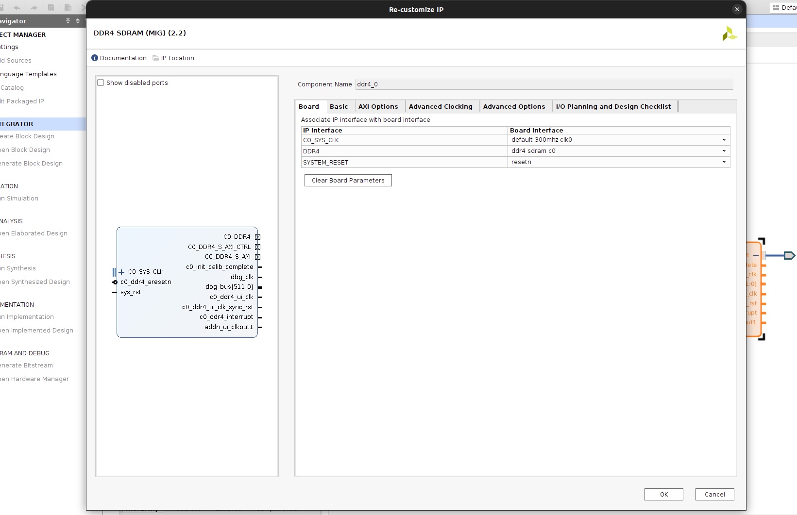
DDR4に生える謎の信号「C0_DDR4_S_AXI_CTRL」を消したい!
C0_DDR4_S_AXIは意味わかるんですけど,C0_DDR4_S_AXI_CTRLはなんなんだ...と混乱.
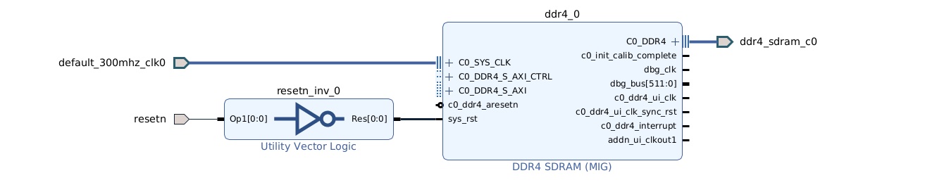
でもプロパティを見ると,生えてない. その信号を消したいのに,元から無いみたいな表示の仕方をされる...
似たようなことをしたい人を発見
Xilinxのコミュニティの投稿
https://support.xilinx.com/s/question/0D52E00006hpOKiSAM/kcu1500-ddr4-interface-question?language=ja
Hi,
I notice that the KCU1500 board has 4 DDR ranks (each 4 GB in size). The DDR4 SDRAM C1 9highlighted in the picture) does not have a C0_DDR4_S_AXI_CTRL interface while other three have the AXI_CTRL (AXI Lite) interface.
Can somehow tell me why?
Also, if I want to use just one rank then which one should I use?
Also, if I want to use all 4 ranks then how should the address map look like?
とのこと.Alveoではないけど,似たことをしたい人がいた.
Xilinxのコミュニティの回答
回答はこんな感じ.
Per UG1260 the 3 interfaces C0, C2 and C3 are 72-bit wide with ECC and interface C1 is 64-bits wide non-ECC. The CTRL interface is available when ECC is enabled.
The information for the ECC status and control registers on the AXI Lite interface can be found in PG150 starting on page 149.
回答の通り確認していく.
KCU1500のDDR4x4のうち,1つだけECC無しらしい
まずUG1260:KCU1500 Board User Guide (UG1260)を見てみると,p.7にこんなことが書かれていた.
Memory (four independent single-rank DDR4 interfaces)
16 GB DDR4 memory
- 3x DDR4 4GB, 2400MT/s, 64-bit w/ ECC
- 1x DDR4 4GB, 2400MT/s, 64-bit w/ no ECC
なるほど,たしかに1つだけno ECCだ.
CTRL interfaceでECCをオフにできるらしい
次にPG150:UltraScale Architecture-Based FPGAs Memory IP v1.4のp.149を確認すると,ECCについての記述があった.
ECC_ON_OFF
The ECC On/Off Control register allows the application to enable or disable ECC checking.The design parameter, C_ECC_ONOFF_RESET_VALUE (default on) determines the reset value for the enable/disable setting of ECC. This facilitates start-up operations when ECC might or might not be initialized in the external memory. When disabled, ECC checking is disabled for read but ECC generation is active for write operations.
まず,C_ECC_ONOFF_RESET_VALUEというデザインパラメータがあるらしい.
これはデフォルトだとonになっているらしく,これを制御することでECCをオフにできるとのこと.
さらに下にはこんなことが
ECC On/Off Control Register
| Bits | Name | Core Acess | Reset Value |
|---|---|---|---|
| 0 | ECC_ON_OFF | R/W | Specified by design parameter, C_ECC_ONOFF_RESET_VALUE |
そしてDescriptionは以下の通り.
If 0, ECC checking is disabled on read operations. (ECC generation is enabled on write operations when C_ECC = 1). If 1, ECC checking is enabled on read operations. All correctable and uncorrectable error conditions are captured and status is updated.
ひとまず C_ECC_ONOFF_RESET_VALUE を0にできればいいらしい.
Alveoでも同じ方法を使えないか探す
Virtex UltraScale+ FPGAに関して,ECC_ON_OFFにする方法を探す
先ほど確認したPG150:UltraScale Architecture-Based FPGAs Memory IP v1.4のp.11にはSupported Device FamilyとしてUltraScale+の記述があった.ということは同じ方法かも?
でも C_ECC_ONOFF_RESET_VALUE の操作方法はどこにも書かれていない...
ほんと初心者に優しくないよねえ.
ドキュメントからDDRのECCについての記述を探す
DS962:Alveo U200 および U250 データセンターアクセラレータ カード データシートを読むとp.3に記述があった.
色々省略して,重要な記述だけ抜き出すとこんな感じ.
XCU200 には 3つの SLR、XCU250 には 4 つの SLR が含まれています。どちらのデバイスも、8 GT/s までで動作可能な PCI Express® (Gen3) の 16 レーンに 接続されます。どちらのデバイスも、エラー訂正符号 (ECC) を含む 16 GB、2400 MT/s、64 ビットの DDR4 DIMM 4 つに接続され、合計 64 GB の DDR4 を提供します。
ということは,AlveoU250のDDR4にはECCが全てについている ってことで,逆にいうとAXI_CTRLは消せない ってことか????
結局「未解決,AXI_CTRLは消せないかも?」
結局よくわからん.けどAXI_CTRLは消せないって可能性が高いと思っている.
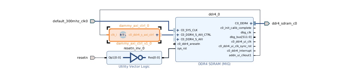
諦めて,AXI_CTRLにダミーのモジュールを作って繋げた
次のようなダミーのモジュールを作ってAXI_CTRLくんに繋げたった.
|
|
いつか無くしたいわねえ.